


Intel’s groundbreaking 8008 microprocessor was first produced over 50 years in the past. This was Intel’s first 8-bit microprocessor and the ancestor of the x86 processor household that you could be be utilizing proper now. I could not discover good die photographs of the 8008, so I opened one up and took some detailed pictures. These new die photographs are on this article, together with a dialogue of the 8008’s inside design.
The picture under exhibits the tiny silicon die contained in the 8008 bundle (click on for increased decision picture). You may barely see the wires and transistors that make up the chip. The squares across the outdoors are the 18 pads which are related to the exterior pins by tiny bond wires.

You may see the textual content “8008” on the precise fringe of the chip and “© Intel 1971” on the decrease edge. The initials HF seem on the highest proper for Hal Feeney, who did the chip’s logic design and bodily structure. Different key designers of the 8008 had been Ted Hoff, Stan Mazor, and Federico Faggin.
Contained in the chip
The diagram under highlights among the main useful blocks of the chip. On the left is the 8-bit Arithmetic/Logic Unit (ALU), which performs the precise knowledge computations.3
The ALU makes use of two non permanent registers to carry its enter values. These registers take up important space on the chip, not as a result of they’re advanced, however as a result of they want giant transistors to drive alerts by way of the ALU circuitry.

Beneath the registers is the carry look forward circuitry. For addition and subtraction, this circuit computes all eight carry values in parallel to enhance efficiency.2 For the reason that low-order carry is determined by simply the low-order bits, whereas the higher-order carries rely on a number of bits, the circuit block has a triangular form.
The triangular structure of the ALU is uncommon. Most processors stack the circuitry for every bit into a daily rectangle (a bit-slice structure). The 8008, nonetheless, has eight blocks (one for every bit) organized haphazardly to suit across the house left by the triangular carry generator. The ALU helps eight easy operations.3
Within the heart of the chip is the instruction register and the instruction decoding logic that determines the that means of every 8-bit machine instruction. Decoding is finished with a Programmable Logic Array (PLA), an association of gates that matches bit patterns and generates the suitable management alerts for the remainder of the chip. On the precise are the storage blocks. The 8008’s seven registers are within the higher proper. Within the decrease proper is the deal with stack, which consists of eight 14-bit deal with phrases. In contrast to most processors, the 8008’s name stack is saved on the chip as a substitute of in reminiscence. This system counter is only one of those addresses, making subroutine calls and returns quite simple. The 8008 makes use of dynamic reminiscence for this storage
The bodily construction of the chip could be very near the block diagram within the 8008 Person’s Guide (under), with blocks situated on the chip in practically the identical positions as within the block diagram.

The construction of the chip
What does the die picture present? For our functions, the chip may be considered three layers. The diagram under exhibits a closeup of the chip, stating these layers. The topmost layer is the metallic wiring. It’s the most seen function, and appears metallic (not surprisingly). Within the element under, these wires are principally horizontal. The polysilicon layer is under the metallic and seems orange beneath the microscope.

The inspiration of the chip is the silicon wafer, which seems purplish-gray within the picture. Pure silicon is successfully an insulator. Areas of it are “doped” with impurities to create semiconducting silicon. Being on the underside, the silicon layer is troublesome to tell apart, however you’ll be able to see black strains alongside the border between doped silicon and undoped silicon. A number of vertical silicon “wires” are seen within the picture.4
Transistors are the important thing part of the chip, and a transistor is fashioned the place a polysilicon wire crosses doped silicon. Within the picture, the polysilicon seems as a brighter orange the place it types a transistor.
Why an 18 pin chip?
One inconvenient function of the 8008 is it solely has 18 pins, which makes the chip slower and rather more troublesome to make use of. The 8008 makes use of 14 deal with bits and eight knowledge bits so with 18 pins there aren’t sufficient pins for every sign. As an alternative, the chip has 8 knowledge pins which are reused in three cycles to transmit the low deal with bits, excessive deal with bits, and knowledge bits. A pc utilizing the 8008 requires many help chips to work together with this inconvenient bus structure.5
There was no good cause to power the chip into 18 pins. Packages with 40 or 48 pins had been widespread with different producers, however 16 pins was “a faith at Intel”.6 Solely with nice reluctance did they transfer to 18 pins. By the point the 8080 processor got here out a number of years later, Intel had come to phrases with 40-pin chips. The 8080 was rather more standard, partially as a result of it had an easier bus design permitted by the 40-pin bundle.
Energy and knowledge paths within the chip
The information bus offers knowledge movement by way of the chip. The diagram under exhibits the 8-bit knowledge bus of the 8008 with rainbow colours for the 8 knowledge strains. The information bus connects to the 8 knowledge pins alongside the skin of the higher half of the chip. The bus runs between the ALU on the left, the instruction register (higher heart), and the registers and stack on the precise. The bus is break up on the left with half alongside either side of the ALU.
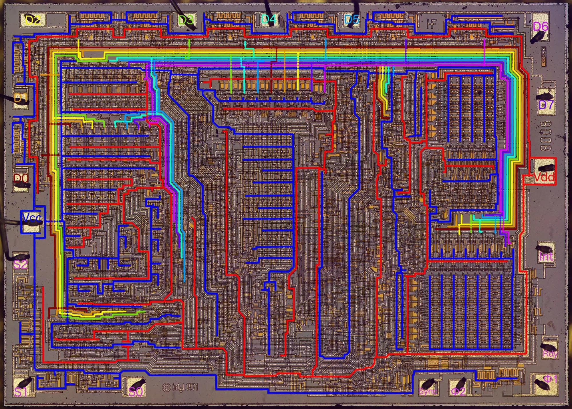
The purple and blue strains present energy routing. Energy routing is an under-appreciated facet of microprocessors. Energy is routed within the metallic layer attributable to its low resistance. However since there is just one metallic layer in early microprocessors, energy distribution have to be rigorously deliberate so the paths do not cross.7 The diagram above exhibits Vcc strains in blue and Vdd strains in purple. Energy is provided by way of the Vcc pin on the left and the Vdd pin on the precise, then branches out into skinny, interlocking wires that provide all elements of the chip.
The register file
To point out what the chip appears like intimately, I’ve zoomed in on the 8008’s register file within the picture under. The register file consists of an 8 by 7 grid of dynamic RAM (DRAM) storage cells, every utilizing three transistors to carry one bit.8 (You may see the transistors because the small rectangles the place the orange polysilicon takes on a barely extra vivid colour.) Every row is among the 8008’s seven 8-bit registers (A, B, C, D, E, H, L). On the left, you’ll be able to see seven pairs of horizontal wires: the learn choose and write choose strains for every register. On the high, you’ll be able to see eight vertical wires to learn or write the contents of every bit, together with 5 thicker wires to provide Vcc. Utilizing DRAM for registers (reasonably than the extra widespread static latches) is an attention-grabbing selection. Since Intel was major a reminiscence firm on the time, I count on they selected DRAM attributable to their experience within the space.

How PMOS works
The 8008 makes use of PMOS transistors. To simplify barely, you’ll be able to consider a PMOS transistor as a change between two silicon wires, managed by a gate enter (of polysilicon). The change closes when its gate enter is low and it may possibly pull its output excessive. If you happen to’re accustomed to the NMOS transistors utilized in microprocessors just like the 6502, PMOS could also be a bit complicated as a result of the whole lot is backwards.
A easy PMOS NAND gate may be constructed as proven under. When each inputs are excessive, the transistors are off and the resistor pulls the output low. When any enter is low, the transistor will conduct, connecting the output to +5. Thus, the circuit implements a NAND gate. For compatibility with 5-volt TTL circuits, the PMOS gate (and thus the 8008) is powered with uncommon voltages: -9V and +5V.

For technical causes, the resistor is definitely applied with a transistor. The diagram under exhibits how the transistor is wired to behave as a pull-down resistor. The element on the precise exhibits how this circuit seems on the chip. The -9V metallic wire is on the high, the transistor is within the center, and the output is the silicon wire on the backside.

Historical past of the 8008
The 8008’s difficult story begins with the Datapoint 2200, a preferred laptop launched in 1970 as a programmable terminal. (Some folks think about the Datapoint 2200 to be the primary private laptop.) Somewhat than utilizing a microprocessor, the Datapoint 2200 contained a board-sized CPU construct from particular person TTL chips. (This was the usual technique to construct a CPU within the minicomputer period.) Datapoint and Intel determined that it might be doable to exchange this board with a single MOS chip, and Intel began the 8008 challenge to construct this chip. A bit later, Texas Devices additionally agreed to construct a single-chip processor for Datapoint. Each chips had been designed to be suitable with the Datapoint 2200’s 8-bit instruction set and structure.

Round March 1971, Texas Devices accomplished their processor chip, calling it the TMC 1795. After delaying the challenge, Intel completed the 8008 chip later, across the finish of 1971. For a wide range of causes, Datapoint rejected each microprocessors and constructed a sooner CPU primarily based on newer TTL chips together with the 74181 ALU chip.
TI tried unsuccessfully to market the TMC 1795 processor to firms resembling Ford, however ended up abandoning the processor, specializing in highly-profitable calculator chips as a substitute. Intel, however, marketed the 8008 as a general-purpose microprocessor, which ultimately led to the x86 structure you are in all probability utilizing proper now. Though TI was first with the 8-bit processor, it was Intel who made their chip successful, creating the microprocessor trade.

The diagram above summarizes the “household tree” of the 8008 and a few associated processors.10 The Datapoint 2200’s structure was used within the TMC 1795, the Intel 8008, and the following model Datapoint 220011. Thus, 4 fully totally different processors had been constructed utilizing the Datapoint 2200’s instruction set and structure. The Intel 8080 processor was a much-improved model of the 8008. It considerably prolonged the 8008’s instruction set and reordered the machine code directions for effectivity. The 8080 was utilized in groundbreaking early microcomputers such because the Altair and the Imsai. After engaged on the 4004 and 8080, designers Federico Faggin and Masatoshi Shima left Intel to construct the Zilog Z-80 microprocessor, which improved on the 8080 and have become highly regarded.
The soar to the 16-bit 8086 processor was a lot much less evolutionary. Most 8080 meeting code might be transformed to run on the 8086, however not trivially, because the instruction set and structure had been radically modified. Nonetheless, some traits of the Datapoint 2200 nonetheless exist in as we speak’s x86 processors. As an illustration, the Datapoint 2200 had a serial processor, processing bytes one bit at a time. For the reason that lowest bit must be processed first, the Datapoint 2200 was little-endian. For compatibility, the 8008 was little-endian, and that is nonetheless the case in Intel’s processors. One other function of the Datapoint 2200 was the parity flag, since parity calculation was vital for a terminal’s communication. The parity flag has continued to the x86 structure.
The 8008 is architecturally unrelated to Intel’s 4-bit 4004 processor12. The 8008 will not be an 8-bit model of the 4-bit 4004 in any manner. The same names are purely a advertising invention; throughout its design part the 8008 had the unexciting identify “1201”.
If you would like extra early microprocessor historical past, I wrote an in depth article for the IEEE Spectrum. I additionally wrote a publish about TI’s TMC 1795.
How the 8008 suits into the historical past of semiconductor know-how
The 4004 and 8008 each used silicon-gate enhancement-mode PMOS, a semiconductor know-how that was solely used briefly. This places the chips at an attention-grabbing level in chip fabrication know-how.
The 8008 (and fashionable processors) makes use of MOS transistors. These transistors had an extended path to acceptance, being slower and fewer dependable than the bipolar transistors utilized in most computer systems of the Sixties. By the late Sixties, MOS built-in circuits had been turning into extra widespread; the usual know-how was PMOS transistors with metallic gates. The gates of the transistor consisted of metallic, which was additionally used to attach parts of the chip. Chips basically had two layers of performance: the silicon itself, and the metallic wiring on high. This know-how was utilized in many Texas Devices calculator chips, in addition to the TMC 1795 chip (the chip that had the identical instruction set because the 8008).
A key innovation that made the 8008 sensible was the self-aligned gate – a transistor utilizing a gate of polysilicon reasonably than metallic. Though this know-how was invented by Fairchild and Bell Labs, it was Intel that pushed the know-how forward. Polysilicon gate transistors had significantly better efficiency than metallic gate (for advanced semiconductor causes). As well as, including a polysilicon layer made routing of alerts within the chip a lot simpler, making the chips denser. The diagram under exhibits the good thing about self-aligned gates: the metal-gate TMC 1795 is larger than the 4004 and 8008 chips mixed.

Shortly afterwards, semiconductor know-how improved once more with the usage of NMOS transistors as a substitute of PMOS transistors. Though PMOS transistors had been simpler to fabricate initially, NMOS transistors are sooner, so as soon as NMOS might be fabricated reliably, they had been a transparent win.
NMOS led to extra highly effective chips such because the Intel 8080 and the Motorola 6800 (each 1974). One other know-how enchancment of this time was ion-implantation to vary the traits of transistors. This allowed the creation of “depletion-mode” transistors to be used as pull-up resistors. These transistors improved chip efficiency and diminished energy consumption. Additionally they allowed the creation of chips that ran on customary five-volt provides.13
The mixture of NMOS transistors and depletion-mode pull-ups was used for many of the microprocessors of the late Nineteen Seventies and early Nineteen Eighties, such because the 6502 (1975), Z-80 (1976), 68000 (1979), and Intel chips from the 8085 (1976) to the 80286 (1982).
Within the mid Nineteen Eighties, CMOS took over, utilizing NMOS and PMOS transistors collectively to dramatically cut back energy consumption, with chips such because the 80386 (1986), 68020 (1984) and ARM1 (1985). Now virtually all chips are CMOS.14
As you’ll be able to see, the Nineteen Seventies had been a time of huge adjustments in semiconductor chip know-how. The 4004 and 8008 had been created when the technological functionality intersected with the precise market.
Learn how to take die photographs
On this part, I clarify how I obtained the photographs of the 8008 die. Step one is to open the chip bundle to reveal the die. Most chips are available in epoxy packages, which may be dissolved with harmful acids.

Since I might reasonably keep away from boiling nitric acid, I took an easier method. The 8008 can also be out there in a ceramic bundle (above), which I obtained on eBay. Tapping the chip alongside the seam with a chisel pops the 2 ceramic layers aside. The picture under exhibits the decrease half of the ceramic bundle, with the die uncovered. Many of the metallic pins have been eliminated, however their positions within the bundle are seen. To the precise of the die is a small sq.; this connects floor (Vcc) to the substrate. A few the tiny bond wires are nonetheless seen, related to the die.

As soon as the die is uncovered, a microscope can be utilized to take pictures. An ordinary microscope shines the sunshine from under, which does not work nicely for die pictures. As an alternative, I used a metallurgical microscope, which shines the sunshine from above to light up the chip.
I took 48 pictures by way of the microscope after which used the Hugin stitching software program to mix them into one high-resolution picture (particulars). Lastly, I adjusted the picture distinction to make the chip’s constructions extra seen. The unique picture (which is roughly what you see by way of the microscope) is under for comparability.

Conclusion
I took detailed die photographs of the 8008 that reveal the circuitry it used. Whereas the 8008 wasn’t the primary microprocessor and even the primary 8-bit microprocessor, it was really revolutionary, triggering the microprocessor revolution and resulting in the x86 structure that dominated private computer systems for many years to return. In future posts, I plan to elucidate the 8008’s circuits intimately to supply a glimpse into the roots of as we speak’s computer systems.
I announce my newest weblog posts on Twitter, so observe me at kenshirriff. Or you need to use the RSS feed.